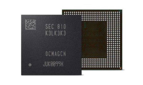
JEDEC Solid State Technology Association has finally announced the publication of JESD209 LPDDR5. It will eventually operate at 6400 MT/s I/O rate, 50% higher than the first version of LPDDR4, which will significantly boost memory speed and efficiency for a variety of applications including mobile computing devices such as smartphones, tablets, and ultra-thin notebooks.
Additionally, LPDDR5 offers new features designed for mission-critical applications such as automotive. Developed by JEDEC’s JC-42.6 Subcommittee for Low Power Memories, LPDDR5 is available for download from the JEDEC website. To achieve significant performance improvement, LPDDR5 architecture was redesigned; moving to 16Banks programmable architecture and multi-clocking architecture.
LPDDR5 introduces two new command-based operations to improve system power consumption by reducing data transmission: Data-Copy and Write-X. The Data-Copy command instructs the LPDDR5 device to copy data transmitted on a single I/O pin to the other I/O pins. The Write-X command instructs the device to write all-ones or all-zeros to a specific address, eliminating the need to send data from the SoC to the LPDDR5 device. Reducing data transmission with these new commands will help reduce overall system power consumption.
To address the need for data reliability in adjacent markets such as automotive, LPDDR5 introduces the support of Link Error Correcting Code (ECC) on the interface between the SoC and DRAM. It comes with WCK & Read Strobe (RDQS) clocking architecture and added to support the higher data rate. The Low-power features added include dynamic Frequency and Voltage Scaling for Core and I/O, selectable differential and single-ended CK, WCK, and RDQS, partial array self-refresh and auto-refresh, and low power read/write operation with Data-Copy and Write-X functions.
